What Is SDRAM? Synchronous Dynamic Random-Access Memory Explained
What is SDRAM?
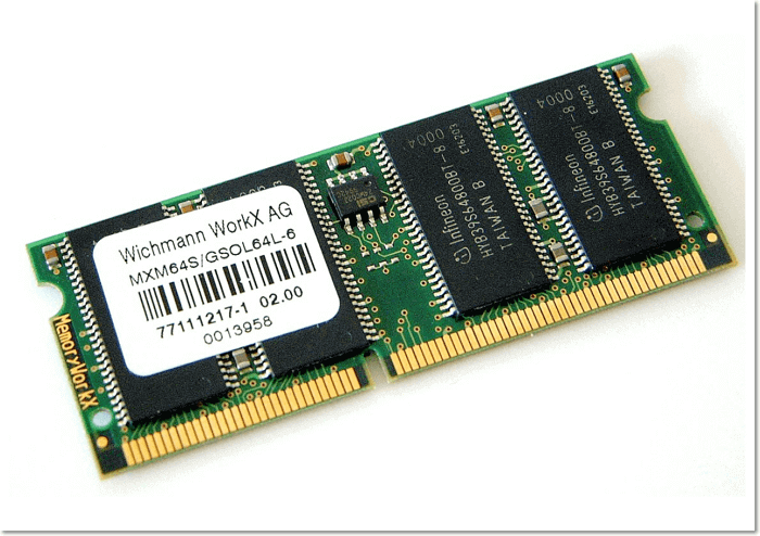
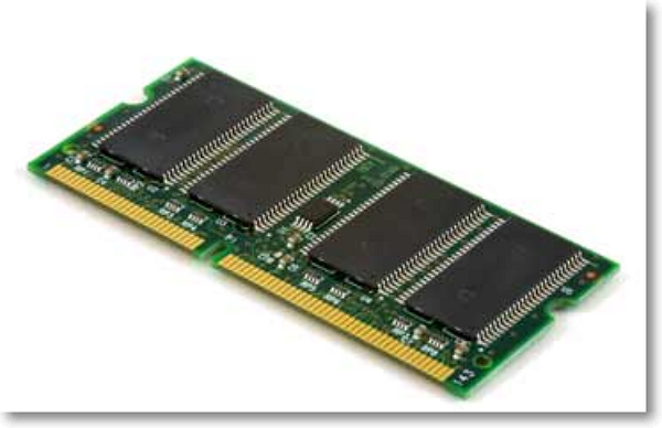
The Synchronous Dynamic Random Access Memory, commonly abbreviated as SDRAM, is a type of dynamic random access memory (DRAM). SDRAM is the form of RAM frequently seen in most computers that provides faster speed when compared to regular DRAM.
The functional operations of SDRAM were first introduced in the 1990s. Before this, processors featured an asynchronous interface, resulting in delayed input control signals due to the trip across the semiconductor pathways. In contrast, the SDRAM integrated circuits use an external clock signal to synchronize the operation of its external pin interface.
The interface of SDRAM is synchronous with the system bus transmitting information from the CPU to the memory controller hub. This results in rapid responses in sync with the system bus, a major contributor to the widespread popularity and use of SDRAM in most computer devices.
Compared to conventional asynchronous DRAMs, SDRAMs offer greater data transfer rates and concurrency. Besides this, SDRAM provides a simple design at a low cost, which can greatly benefit manufacturers. These advantages have made SDRAM a popular and preferred choice in the computer memory market, particularly for RAM.

Development of SDRAM
With the passage of years, SDRAM has evolved into many generations, each with its functional capabilities. Here is a brief overview of SDRAM's development over the decades leading up to its latest generation.
DDR (1st Generation)
The first generation of SDRAM, known as DDR (Double Data Rate) SDRAM, preceded SDR interfaces. DDR provides more strict control of phasing the clock signals and thus results in greater transfer rates.
Another notable feature of the DDR interface is double pumping, which allows the transfer of data on both edges of the clock cycle, making it possible to double the bandwidth of the data bus. This also prevents the clock frequency from getting too high, so the signal integrity requirements can be kept down.
The clock rate on DDR falls between 133 and 200 MHz, with a prefetch butcher size of 2n (two data words per memory access). The data transfer rate for DDR is 2.1-3.2 GB/s, and the operational voltage is 2.5/2.6.
DDR2 (2nd Generation)
The Double Data Rate 2 SDRAM was first seen in 2001 by Samsung, succeeding the first generation of DDR SDRAM. In later years, DDR2 was offered with two clock rates: 200 and 266MHz. Compared to its predecessor, DDR2 offered an increased prefetch length of four bits for every bit in a word.
By increasing the prefetch length, DDR2 provides almost double the data transfer rate over the data bus. The main idea behind DDR2 was to do this without a boost in the processor's power consumption. Despite this, DDR2 saw a spike in memory latency between three and nine cycles.
The highest recommended voltage for DDR2 was 1.9V, with a bus clock of 266-400MHz. DDR2 allows a data transfer rate of 4.2-6.4 GB/s and is not backward compatible with DDR modules due to its higher pin density of 240 compared to the 184-pin modules seen in DDR.
DDR3 (3rd Generation)
The 3rd generation of double data rate SDRAM, abbreviated as DDR3, has been seen in devices since 2007. DDR3 features distinct signaling voltages and timings, due to which it is not forward or backward compatible with any of its predecessor RAMs.
The prefetch butcher size in DDR3 is double that of DDR2, an 8n length that allows up to eight times the data transfer speed. This has enabled DDR3 to provide greater data transfer rates and higher bandwidths.
The maximum voltage that DDR3 can endure is between 1.35 and 1.5V, and the transfer rates fall between 8.5-14.9 GB/s.
DDR4 (4th Generation)
DDR3 was succeeded by the 4th generation of double data rate SDRAM, DDR4, in 2014. It is significantly different than other earlier RAM types in terms of the physical interface, signaling voltages, and other factors. As a result, DDR4 is incompatible with any of its predecessors and offers a data transfer rate of 8.5-14.9 GB/s.
Compared to previous generations of DDR SDRAMs, DDR4 offers higher module density and data transfer speeds, all at lower voltages (up to 1.2V at frequencies between 800 and 1600 MHz). The prefetch length in DDR4 is the same as DDR3 (8n), and the DRAM banks have been divided into two or four selectable groups to allow higher bandwidths.
DDR5 (5th Generation)
Released in 2020, the latest generation of double data rate SDRAM is the DDR5. While offering the same prefetch butcher size and latency as DDR3 and DDR4, the fifth generation of SDRAM supports a bandwidth of 4.8 GB/s. The DDR5 has also seen a further voltage drop, reaching up to 1.1V.
The highest speed offered by DDR5 was 6400 MT/s released in 2019 by SK Hynix, whereas Samsung released a 512 GB 7200 MHz DDR5 DIMM in 2021. DDR5 allows up to eight bank groups with a maximum of four banks per group, allowing greater bandwidths.

SDRAM vs. DDR
At this point, you are aware of the basics of SDRAM. Followed by the generational discussion, you may now tend to look ahead into discussing some of the prime differences that make these different from each other. We will be taking SDRAM and DDR for this case and will feature a coherent table showing the major differences among them:
| SDRAM | DDR |
|---|---|
| It was released in 1997 for commercial use. | Introduced in 2000 for commercial computing utility. |
| Operates on a voltage of 3.3V. | Works perfectly within the range of 1.8-2.5V. |
| Contains 168 pins and 2 notches across the connector. | Contains 184 pins and one notch across the connector for enhanced operations. |
| Offers prefetch timing of 1ns. | Prefetch timing is improved to 2ns. |
| Features a data rate of 0.8-1.3 GB/s. | Provides a data rate approximately double the value at 2.1-3.2 GB/s. |
| Provides an internal rate range of 100MHz – 166MHz. | Covers an internal rate range of 133MHz – 200MHz. |
| Lesser speed in comparison to DDR. | Provides a speed that is almost double as compared to SDRAM's speed. |
Conclusion
SDRAM is a type of memory used on integrated circuits that has gained extreme popularity since its release. Owing to its fast speed and synchronous interface, SDRAM has replaced DRAM in most computer devices. The latest generation of SDRAM, DDR5, offers higher bandwidth at significantly lower power consumption.
Related Articles
- What Is the SysWOW64 Folder? SysWOW64 vs System32
- What Is System Partition? [Best Explained in 2022]
- [Beginner Guide] What Is PCIe? What Is It Used for?
- MTS File : What Is It and How To Open It [Updated 2022]